Asynchronous Register Less NULL Convention Logic (RL-NCL) Pipeline
Architectures Using Basic Gates
Arquitecturas Pipeline
Asincrónicas Register Less NULL
Convention Logic (RL-NCL)
Usando Puertas Básicas
Arquiteturas de Pipeline
Assíncronas Register Less NULL Convention Logic (RL-NCL) Usando Portas Básicas
Gabriel C. Duarte [1], Duarte L. Oliveira [2]
Recibido: Mayo
2022 Aceptado:
Octubre 2022
Summary. - Asynchronous
circuits is an alternative to design digital systems that is becoming the
interest of many researchers in the digital design area mainly due to it’s
low-power consumption and robustness. One of the most compelling design
paradigms of asynchronous circuits is the NULL Convention Logic (NCL). The
pipeline is a very common technique used in digital circuits to achieve high
throughput. Although one can implement a pipeline using NCL gates, recent works
have shown that register-less pipelines are possible using modified NCL gates.
In this paper we propose two new Register-Less NCL (RL-NCL) pipeline
architectures and two new methods to design NCL gates, which can be implemented
even in Field Programmable Gate Arrays (FPGAs) or using the standard cells
method. The new design of the proposed architecture was able to achieve an
average area reduction of 27,32%, an average latency reduction of 14,1% and an
average throughput increase of 5,54% comparing with the conventional NCL
pipeline architecture.
Keywords:
Asynchronous Circuits; NCL;
RL-NCL; FPGA; Pipeline.
Resumen.
- Los circuitos
asíncronos son una alternativa para el diseño de sistemas digitales que se está
convirtiendo en el interés de muchos investigadores en el área del diseño
digital debido principalmente a su bajo consumo y robustez. Uno de los
paradigmas de diseño más convincentes de los circuitos asíncronos es la NULL
Convention Logic (NCL). La pipeline es una técnica muy común utilizada en
circuitos digitales para lograr un alto rendimiento. Aunque se puede
implementar una pipeline utilizando puertas NCL, trabajos recientes han
demostrado que las pipelines sin registro son posibles utilizando puertas NCL
modificadas. En este artículo, propusimos dos nuevas arquitecturas de pipeline
Register-Less NCL (RL-NCL) y un paradigma de diseño, que pueden implementarse
incluso en Field Programmable Gate Arrays (FPGA) o utilizando el método de
celdas estándar. El nuevo diseño de la arquitectura propuesta logró una
reducción media del área del 27,32%, una reducción media de la latencia del
14,1% y un aumento medio del rendimiento del 5,54% en comparación con la
arquitectura de pipeline NCL convencional.
Palabras clave: Circuitos Asíncronos; NCL; RL-NCL; FPGA;
Pipeline
Resumo. - Circuitos assíncronos é uma alternativa para projetar
sistemas digitais que vem despertando o interesse de muitos pesquisadores na
área de projeto digital principalmente devido ao seu baixo consumo de energia e
robustez. Um dos paradigmas de projeto mais atraentes de circuitos assíncronos
é o NULL Convention Logic (NCL). O pipeline é uma técnica muito comum usada em
circuitos digitais para obter alto rendimento. Embora seja possível implementar
um pipeline usando portas NCL, trabalhos recentes mostraram que pipelines sem
registro são possíveis usando portas NCL modificadas. Neste artigo propomos
duas novas arquiteturas de pipeline NCL Register-Less (RL-NCL) e dois novos
métodos para projetar portas NCL, que podem ser implementadas até mesmo em
Field Programmable Gate Arrays (FPGAs) ou usando o método de células padrão. O
novo design da arquitetura proposta foi capaz de alcançar uma redução média de
área de 27,32%, uma redução média de latência de 14,1% e um aumento médio de
throughput de 5,54% em comparação com a arquitetura de pipeline NCL
convencional.
Palavras-chave: Circuitos assíncronos; NCL; RL-NC; FPGA;
Pipeline
1. Introduction. - This paper is an
extended version of the work originally presented in the 2021 IEEE URUCON
conference [1]. In this work, we added in the experimental simulations 4
circuits from a well-known benchmark, that correspond to a raise of 66,6% in
the number of circuits used in the experimental validation. A new architecture
is also proposed.
With the growing number of transistors being placed
inside Integrated Circuits (IC) nowadays due to the reduction in the size of
this component, synchronous digital systems became more difficult to design
[2]. The distribution of the clock alongside the chip, the clock skew problem
and the fact that the clock frequency and the power consumption are directly
proportional are the main reasons that makes asynchronous digital systems an
interesting alternative and why the interest for this paradigm grows today for
many researchers. Of the most popular research topic nowadays we can cite
artificial intelligence, machine learning and Internet of Things (IoT), in all
of them low power consumption is a key challenge for the designers [3].
Cryptography is an application that already takes the advantages of asynchronous
circuits. Recently, a work showed that the power consumption can be improved
using the NULL Convention Logic asynchronous paradigm to implement cryptography
algorithms, such as the Advanced Encryption Standard (AES) [4].
One famous technique used by digital designers to
raise the throughput of circuits is the pipeline, which divides the circuit
into stages with the insertion of registers to hold partial values.
Asynchronous pipelines have four considerable advantages over synchronous
pipelines [5]: (1) In a synchronous pipeline the clock frequency is calculated
using the critical path of the circuit and all stages operates in the same
rate, while in the asynchronous one, each stage operates accordingly with its
own critical path, reducing the latency time. (2) Asynchronous pipelines can
have a variable number of data at any time, because of this each data is
processed when it’s available, while in the synchronous pipeline a correct
operation requires new data to arrive at predefined timed intervals. (3)
Inherent flow control due to the handshake protocols used by asynchronous
systems. (4) The dynamic power consumption is on demand, only when there is
data to be processed. The circuit is quiescent when there is no data to be processed.
One of the most famous asynchronous paradigms is the
NULL Convention Logic (NCL) framework proposed by [6]. NCL circuits are
implemented using the 27 NCL gates, which consists of every Boolean function of
four or fewer variables. NCL gates are also called threshold gates and have a
state-holding hysteresis capability [7], meaning that once the output of the
gate is set, it will be reseted only when all inputs are reseted. With NCL
gates, Delay-Insensitive (DI) circuits can be implemented using dual-rail or
quad-rail codes, and the design is similar to synchronous circuits. While in
synchronous design the function is mapped to logic gates, in NCL circuits the
function is mapped to a set of NCL gates.
The NCL paradigm also support the pipeline technique
using the TH22 NCL gate to obtain the NCL registers for a dual-rail circuit,
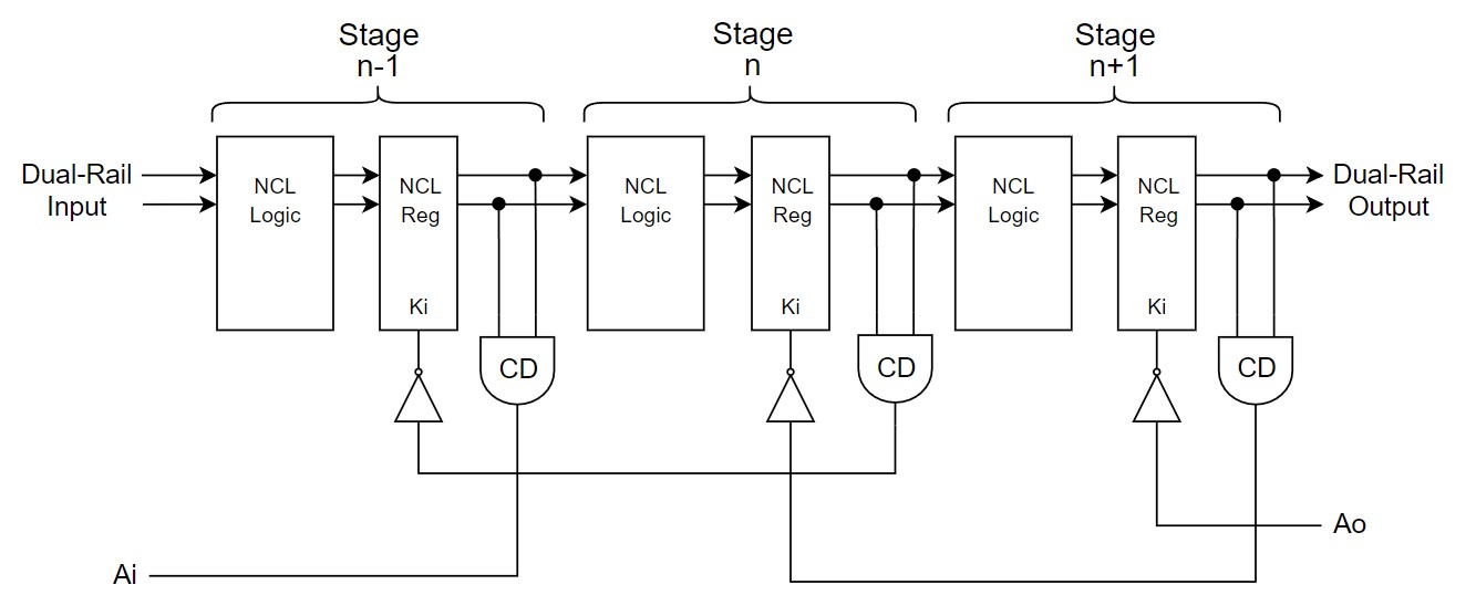
since a TH22 gate operation is identical to a C-element of 2-inputs. Figure I present
the conventional NCL pipeline with three stages for a dual-rail circuit. Each
stage consists of the processing block (composed of NCL gates), NCL registers
to store partial values and the completeness detector (CD) circuit, which
indicates when a new data is available. The acknowledge in (Ai) output
indicates when a data is acknowledged by the first stage, and the acknowledge
out (Ao) input tells when the output of the pipeline was acknowledged. The NCL
pipeline operates in the four-phase handshake protocol.
Even though the NCL pipeline is robust and can be used
in many applications, a recent work [8] have shown that a more efficient
version of this architecture can be obtained, eliminating all registers used by
the pipeline, reducing the area and the power consumption. This architecture is
a Register-Less NCL (RL-NCL) pipeline and uses a modified version of the NCL
paradigm, the Multi-Threshold NCL (MT-NCL) [9]. The MTNCL combines the
Multi-Threshold CMOS (MT-
CMOS) [10] and the NCL paradigm and was initially
proposed by [11]. The MT-NCL gates uses the Sleep signal to keep the respective
gate active or to put in sleep mode, and thus reduce the power consumption.
|
|
|
Figure I: Conventional NCL pipeline. |
By using the MT-NCL gates in the processing blocks of
each stage and with only one C-element per stage, the sleep signal can be used
to control each stage of the RL-NCL pipeline. The only disadvantage of this
architecture is that the project is full custom. Other techniques can be used
to obtain a more efficient pipeline circuit, such as using embedded registers
in the NCL processing logic [7].
Many architectures and methods for the implementation
of NCL gates were proposed in the literature. Although both for
transistor-level and gate-level designs, transistor-level proposals and research
are far more common than gate-level implementation and proposals for the NCL
paradigm. This paper addresses this problem by proposing two new gate-level implementations
of NCL gates with the addition of a control signal, thus allowing a gate-level
implementation of two novel RL-NCL pipeline architectures. The main advantage
of the proposed architectures is that it does not require a full-custom project
and can be implemented in FPGAs or using the standard cells method.
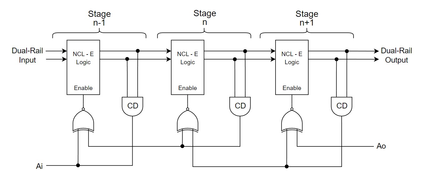
The first proposed pipeline architecture is shown in
Fig. II for a generic 3-stage pipeline. The control circuit is simple and uses
only one gate for each stage. The method to implement NCL gates using basic gates
uses the enable signal to control the operation of the stage, thus we call this
method NCL-E. In the original paper [1] the logic block was inaccurately called
NCLS with the control signal being called sleep, but we changed to NCL-E in
this paper since the sleep signal behavior is different from the behavior of
the proposed method to implement NCL gates.
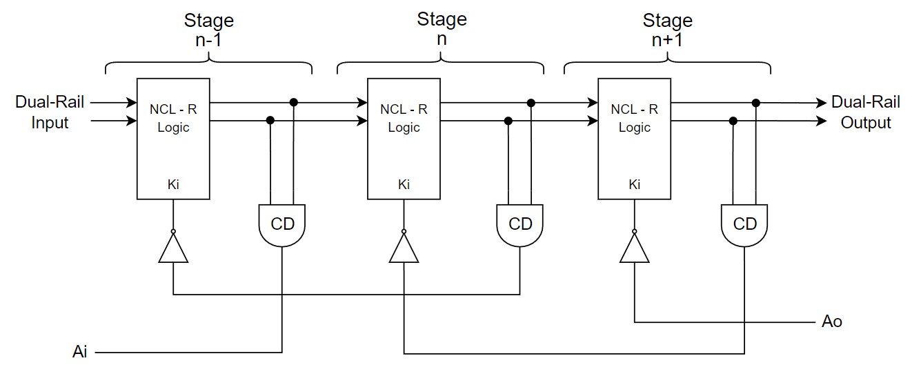
Figure III shows an alternative design of the proposed
RL-NCL pipeline architecture using a new method to implement NCL gates with
embedded registers, which we call NCL-R. The pipeline architecture is similar
to the conventional NCL pipeline, only removing the registers of each stage. It
also does not require any additional circuit for the control of each stage.
The rest of the paper is organized as follows: Section
II present some background in asynchronous circuits, including the NCL
paradigm, the classification of asynchronous circuits regarding the delay
model, the dual-rail code and handshake protocols. In Section III we present the
related works regarding gate-level implementation of NCL gates. Section IV
presents the first proposed new method to implement NCL gates with the addition
of the enable signal and the proposed pipeline architecture presented in Fig.
II, and Section V presents a new alternative design method to implement NCL
gates and the pipeline architecture related to this method and presented in
Fig. III. In Section VI we present the experimental implementation of both
proposed architectures and the conventional NCL pipeline of the literature,
then we show and discuss the simulation results. Finally, in section VII we
make the conclusions about this paper.
|
|
|
Figure II: RL-NCL pipeline architecture using
the enable signal, proposed in [1]. |
|
|
|
Figure III: New design: RL-NCL pipeline
architecture using NCL gates with embedded registers. |
2. Asynchronous Circuits Background. -
Asynchronous circuits can be classified according to its delay model [12]:
Bundled-Data (BD) circuits depends on defined delay values and specific timing
intervals to operate correctly. If the circuit does not respect these intervals
the correct operation cannot be guaranteed. To guarantee a correct operation, matching
delays greater than the delays of critical paths are inserted in the circuit.
Speed-Independent (SI) circuits operates correctly if the delays in the logic
gates are positive, finite and arbitrary, but the delays of the wires must be
zero.
Delay-Insensitive (DI) circuits operates correctly if
both the delays of the gates and of the wires are positive, finite and
arbitrary. Thus, DI sensitive circuits are the most robust class of
asynchronous circuits. The Quasi Delay-Insensitive (QDI) is the most robust
class that can be implemented for the majority of the circuits. QDI circuits
also operates correctly if the delays of the gates and wires are positive,
finite and arbitrary but with an additional restriction: the isochronic forks.
That is, if a wire has a fork, each fork must have the same delays.
To achieve greater robustness, asynchronous circuits use
DI codes, such as the dual-rail and the quad-rail. The most common code for NCL
circuits design is the dual-rail, in which each bit of data is represented with
two wires, the true-rail and the false-rail. A one bit data "a" can
have three values: (1) ![]() : in
this case both rails are zero, so "a" has a NULL value; (2)
: in
this case both rails are zero, so "a" has a NULL value; (2) ![]() :
the false rail is one and the true rail is zero, in this case "a" has
the logic level zero; (3)
:
the false rail is one and the true rail is zero, in this case "a" has
the logic level zero; (3) ![]() :
the true rail is one and the false rail is zero, thus "a" has a logic
level one. Both rails cannot be one at the same time, so the transition from a
valid data to another one has to be separated by a NULL value.
:
the true rail is one and the false rail is zero, thus "a" has a logic
level one. Both rails cannot be one at the same time, so the transition from a
valid data to another one has to be separated by a NULL value.
Asynchronous circuits can operate in the two-phase or
in the four-phase protocol. In the two-phase protocol, once a data is
acknowledged by the receiver a new data can be sent. This is represented by a
wire transition, in both low to high or high to low. In the four-phase
protocol, once a data is acknowledged by the receiver the protocol has to
return to zero, and then a new data can be sent. Due to the nature of each
protocol, dual-rail circuits operate naturally in the four-phase protocol. In
dual-rail circuits a transition from low to high indicates that a valid data
was acknowledged and a transition from high to low indicates that a NULL value
was acknowledged.
3. Related Works. - In the past two
decades the NCL paradigm has grown in interest of many researchers and has
achieved important progress. Most of the NCL gates implementation are targeted
at transistor-level implementation in CMOS technology (such as Static,
Semi-Static and Differential implementations), with recent studies showing
implementations in new technologies such as FinFET and carbon nanotube-FET
(CNTFET). Along with that, the design flow (logic synthesis, optimization and
technology mapping), testing and verification also achieved great progress
[13].
Several gate-level styles for the implementation of
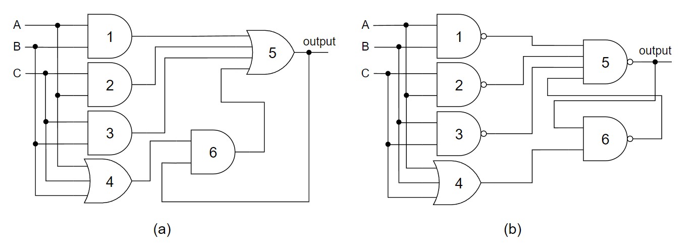
NCL gates were proposed in the literature. As an example, let’s analyze the NCL
TH23 gate (AB+AC+BC) implemented in two proposals. The implementation of the
TH23 gate in the architecture proposed in [14] is presented in Fig IV (a). The
architecture uses an AND gate (gate 6) with the output feedback and the OR
function of the inputs (gate 4) to obtain the hysteresis condition, so once the
output is set, it can only be reseted when all inputs are zero. The output is
obtained with the OR function of the NCL gate function, in this example
implemented by gates 1, 2 and 3, with the output of the hysteresis circuit
(gate 6).
Another method to implement NCL gates using basic
gates is the Standard RS architecture, that uses a standard set-reset (RS)
latch using NAND gates and is based in the static implementation of NCL gates
[15]. The circuit of the TH23 NCL gate implemented using this architecture is
shown in Fig IV (b). The set input of the latch (gate 5) receives the inverted
NCL function, since the latch is set with a logic level zero. Gates 1, 2 and 3
implement the negated NCL function. The reset input of the latch (gate 6)
receives the OR function of the inputs of the NCL gate, so the output only
resets when all inputs are zero. When any of the inputs are different from
zero, the latch retains the previous value. This way the hysteresis condition
of NCL gates is satisfied.
Recently, two new studies analyzed the timing behavior
of the architectures mentioned above and showed that both implementations are
not quasi delay-insensitive (QDI), consequently they have timing restrictions
[16; 17]. The papers also proposed a new architecture for the implementation of
NCL gates that is QDI, thus being more robust.
|
|
|
Figure IV: NCL TH23 gate using: (a)
Architecture of [14] (b) Standard RS Architecture. |
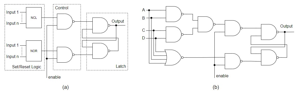
4. Proposed Architecture. - To
achieve the proposed pipeline architecture of the Fig II, a new method to
implement NCL gates is also proposed. Fig. V (a) presents the new method to
implement NCL gates with the addition of the enable signal, similar to a RS
latch with enable. When the enable is equal to a logic one, the latch can set
or reset the output depending on the inputs of the NCL function and when the
enable is equal to a logic zero, the latch keeps the previous value. The
circuit used to set the output is the NCL function itself, and to reset is a
NOR gate with fan-in equal to the number of inputs of the NCL gate. This way,
the circuit will set the output only when the enable is a logic one and the NCL
function is true and will only reset when the enable is one and all the inputs
are zero. As an example, Fig. V (b) shows the NCL THxor0 gate using the
proposed NCL-E method.
|
|
|
Figure V: Proposed NCL-E gate level: (a)
Generic NCL-E gate (b) THxor0. |
Comparing the proposed architecture with an
architecture from the literature [8], besides the main difference that is the
logic block implementation (MTNCL logic that is full-custom and the proposed
NCL-E method that can be implemented with basic gates) the architectures are
similar. Both have a circuit for detecting the completeness of data at the end
of each stage and for the control, one uses a C-element and our proposal uses a
XNOR gate.
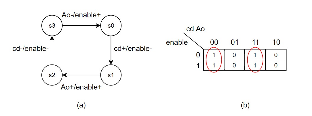
The control circuit for each stage was obtained using
the Burst-Mode (BM) specification [18]. Fig. VI (a) presents the BM specification
for the control circuit and Fig. VI (b) shows the Karnaugh Map of the
specification, which implements a XNOR gate. The signals cd and Ao are the
inputs and the enable is the output that controls the NCL-E gates.
|
|
|
Figure VI: Control circuit: (a) BM Specification
(b) Karnaugh Map. |
The CD circuit can be implemented using the NCL gates
TH12 and TH22, similar to the circuit used in the NCL register or with
conventional OR gates and one C-element at the output. The output of the CD
circuit is a logic one when all the gates have a valid value at its outputs and
zero when all the gates have a NULL value.
The proposed NCL-E gates can also be used in
conjunction with conventional NCL gates at the end of the stage processing
block, in cases where the circuit of a stage has a higher depth of logic
processing.
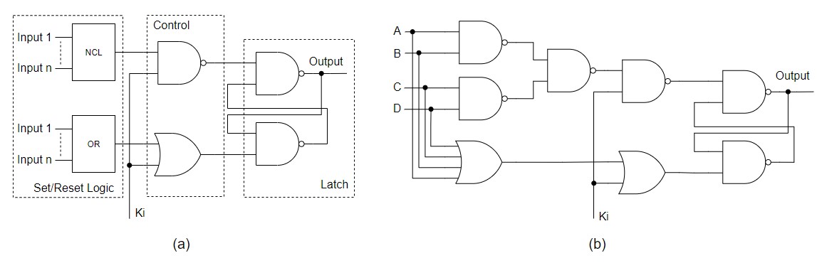
5. Alternative Design: A More Robust Implementation. - For
the alternative pipeline architecture presented in Fig III to work correctly, a
new method to implement NCL gates is also proposed, in which an additional
input is used to control the behavior of the gate. This input is called Ki
because it has a similar role as the Ki input of a NCL register and the main
reason why we choose to call this method a NCL-R circuit is because it behaves
like a NCL gate with an embedded register. The circuit used to implement the
NCL gates in the proposed method is shown in Fig. VII (a) and is divided in
three parts: The latch, the control block and the set/reset logic.
The latch block is a standard RS latch using NAND
gates. The control block is similar to the additional circuit used to enable a
RS latch with a little modification, since the enable signal and the Ki signal
have different behaviors. A conventional RS latch with enable is only set or
reset when the enable is a logic one. On the other hand, when the Ki signal is
a logic one, it must enable the latch to set its output and block the reset
condition and when the Ki signal is a logic zero, it must enable the latch to
be reseted and block the set condition, thus the control block uses a NAND gate
for the set signal and an OR gate for the reset signal of the latch. The
set/reset logic block depends on the NCL gate to be implemented. The reset
condition is obtained with one OR gate with fan-in equal to the number of
inputs of the desired NCL gates, so the output of the OR gate is zero only when
all inputs are zero and consequently guaranteeing the hysteresis condition of
only reseting the output when all inputs are zero. The set condition is the NCL
function itself.
As an example, we choose to present the NCL THxor0
gate using the proposed method. Fig. VII (b) shows the circuit of the THxor0
gate in the proposed method. The NCL block is implemented using the three NAND
gates that implement the logic function AB+CD of the THxor0 gate. The reset
logic is the OR gate with fan-in equal to four that receives the inputs A, B, C
and D. When the Ki signal is logic one it will enable the output to be set
waiting on the NCL function. Once the output is set, it will only be reseted
when the Ki signal is zero and all the inputs of the NCL gate are also zero.
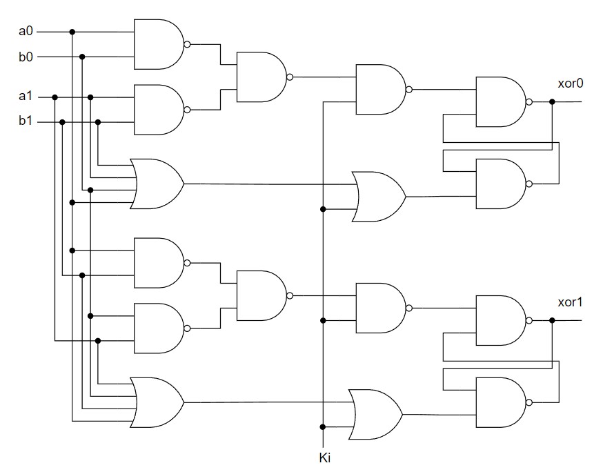
Fig VIII show a dual-rail 2-input XOR gate in the proposed NCL-R method.
|
|
|
Figure VII: Proposed NCL-R gate level: (a)
Generic NCL-R gate (b) THxor0. |
|
|
|
Figure VIII: Dual-rail 2-input XOR gate in
the proposed NCL-R method. |
6. Experimental Results and Discussion. - To
validate the correct operation of the proposed method to implement the NCL
gates and the new RL-NCL architectures, we implemented ten circuits in FPGA
both in the proposed architectures and in the conventional NCL pipeline for
performance comparison.
All the circuits were described in structural VHDL and
synthesized for the Intel Cyclone IV family’s EP4CE115F29 device in the Quartus
Software. This device was chosen because it’s the FPGA that is in the Altera
DE2-115 development and educational board, used in many universities over the
world. The post-synthesis (timing) simulations were performed in the ModelSim
software. To compare the performance of each pipeline we used four parameters:
(1) Latency (in nanoseconds), the time needed for a new data to cross all the
stages of the pipeline and be available at the output. (2) Throughput, in
million operations per seconds (MOPS). (3) Dynamic power con-
|
Parameter |
Arch. |
ALU |
KSA |
Mult. |
Prim. |
Pari. |
Comp. |
c17 |
cm82 |
cm152 |
majo. |
|
LUTs |
NCL NCL-E |
111 94 |
537 475 |
147 123 |
57 41 |
100 72 |
156 112 |
72 52 |
143 103 |
156 112 |
128 92 |
|
|
NCL-R |
91 |
465 |
123 |
39 |
67 |
107 |
48 |
96 |
107 |
87 |
|
Power |
NCL NCL-E |
1,1 1,06 |
3,25 3,61 |
1,01 1,1 |
0,44 0,41 |
0,81 0,77 |
1,05 1,03 |
0,54 0,55 |
0,89 0,79 |
1,05 1,06 |
0,84 0,79 |
|
|
NCL-R |
0,95 |
4,65 |
1,23 |
0,64 |
0,79 |
1,31 |
0,52 |
0,88 |
1,22 |
0,94 |
|
Latency |
NCL NCL-E |
15,67 14,33 |
23,13 22,42 |
15,63 16,23 |
11,99 10,27 |
15,93 12,64 |
15,59 12,26 |
12,29 11,59 |
14,83 12,95 |
15,42 12,53 |
15,2 12,62 |
|
|
NCL-R |
14,27 |
21,35 |
13,42 |
10,52 |
13,08 |
13,61 |
8,48 |
13,8 |
13,29 |
12,81 |
|
Throughput |
NCL NCL-E |
25,81 23,15 |
15,46 16,28 |
18,63 20,06 |
21,47 22,87 |
20,41 20,41 |
16,6 18,23 |
21,11 22,18 |
19,68 20,79 |
16,61 17,53 |
17,97 18,98 |
|
|
NCL-R |
24,88 |
17,28 |
21,99 |
21,83 |
20,72 |
16,74 |
22,83 |
21,05 |
17,79 |
18,55 |
Table I: Simulation Results
sumption, measured in milliWatts (mW) and (4) the
required area used by the circuits, in this case measured in number of LUTs. To
obtain the power consumption, all the simulations performed generated the .vcd
file which specifies all the transitions in the circuit and was used in the
PowerPlay tool, which is integrated in the Quartus software.
We choose six common digital circuits to implement in
both architectures along with four circuits obtained from the LGSynth91
benchmark [19], which is one of the ACM/SIGDA benchmarks. The six common
digital circuits are: ALU, array multiplier, prime number detector, parity
detector, comparator and a Kogge-Stone Adder (KSA). The four benchmark circuits
are: c17, cm82a, cm152a and majority. Table I shows the obtained results of
each circuit in both pipelines for each parameter mentioned above.
The proposed NCL-E architecture obtained better
results in nine out of the ten circuits for the latency time, in eight out of
ten for the throughput and in six out of ten for the dynamic power consumption.
For the area, the proposed architecture obtained better results in all
circuits. In average, the NCL-E architecture obtained a reduction of 12,5%,
1,17% and 23,98% in latency time, power consumption and number of LUTs and
obtained a raise of 4,1% in throughput comparing with the NCL pipeline.
We highlight that the proposed NCL-R architecture
obtained a reduction in the latency time and in area in all ten circuits, with
an average reduction of 14,1% and 27,32%, respectively. The proposed
architecture achieved a throughput raise in nine out of the ten circuits
simulated, with an average increase of 5,54%. As a drawback, the proposed
architecture consumed more dynamic power in six out of the ten circuits with an
average increase of 14,2% in the dynamic power consumption. Although the
proposed architecture consumed more power, the measured values were all
calculated with the circuits operating at the maximum throughput, and a more
detailed power consumption analysis can be made with the circuits operating at
the same throughput for better comparison.
Comparing the NCL-E and the NCL-R architectures, the
NCL-R architecture obtained better results in latency time, throughtput and
area, but as a drawback consumed more power.
7. Conclusion. - With new
requirements for the design of modern circuits, systems and applications, such
as low power consumption and robustness, the asynchronous paradigm is gathering
more attention by the researchers and the NCL circuits is one promising design
choice, being capable of even implementing pipelines without the need of using
registers.
Although there have been important accomplishments and
new works recently in the asynchronous circuits area due to the raising of
interest for this class of circuits, most of the works are targeted to
full-custom projects at the transistor level and much less at the gate-level,
targeting FPGAs or the standard cells method. Along with that, there’s still
much work to be done in Computer-Aided Design (CAD) tools for asynchronous circuits
to make it more relevant for designers.
This paper proposes two new methods to implement NCL
gates using only basic gates, therefore being suitable for FPGA and standard
cells implementations and not requiring a full-custom project. In each new method
to implement NCL gates we introduce a control signal, enable and Ki,
respectively. With the new methods to implement the NCL gates, two new RL-NCL
pipeline architectures are also proposed, with of one of them being very
similar to the conventional NCL pipeline and therefore working without
additional control circuits for each stage. Both new pipeline architectures
obtained a significant area reduction, of 23,98% and 27,32% respectively for
the NCL-E and NCL-R proposals, in comparison with the conventional NCL
pipeline. This was achieved due to the removal of the registers. A reduction in
latency and an increase in throughput was also achieved, showing the viability
and good performance of the proposed architectures. The second proposal was
designed to be a robust implementation of a RL-NCL pipeline, operating exactly
like the NCL pipeline.
For future works, we wish to implement the
architectures in Very Large Scale Integration (VLSI) using the standard cells
method, so a comparison with the other RL-NCL architecture from the literature
can be obtained. Another work to be done is develop a CAD tool to help
designers to obtain an automated process to synthesize circuits in the proposed
RL-NCL architectures. The implementation of the architectures in other FPGA
vendors, such as Xilinx and/or Lattice, for comparison between many FPGA
families and technology implementations, is also another future work to be
accomplished.
8. References. -
[1]
G. C. Duarte and D. L. Oliveira, “A novel asynchronous
pipeline architecture with less-registers using null convention logic,” in 2021 IEEE URUCON, 2021, pp. 36–41.
[2]
B. H. Calhoun, Y. Cao, X. Li, K. Mai, L. T. Pileggi,
R. A. Rutenbar, and K. L. Shepard, “Digital circuit design challenges and
opportunities in the era of nanoscale cmos,” Proceedings of the IEEE, vol. 96, no. 2, pp. 343–365, 2008.
[3]
L. Ye, Z. Wang, Y. Liu, P. Chen, H. Li, H. Zhang, M.
Wu, W. He, L. Shen, Y. Zhang, Z. Tan, Y. Wang, and R. Huang, “The challenges
and emerging technologies for low-power artificial intelligence iot systems,” IEEE Transactions on Circuits and Systems I:
Regular Papers, vol. 68, no. 12, pp. 4821–4834, 2021.
[4]
T. Le Thanh, L. T. Tri, and H. Trang, “Power
consumption improvements in aes decryption based on null convention logic,” International Journal of Circuits, Systems
and Signal Processing, vol. 15, pp. 254–264, 2021.
[5]
S. M. Nowick and M. Singh, “High-performance
asynchronous pipelines: An overview,” Ieee
design & test of computers, vol. 28, no. 5, pp. 8–22, 2011.
[6]
K. M. Fant and S. A. Brandt, “Null convention
logic/sup tm/: a complete and consistent logic for asynchronous digital circuit
synthesis,” in Proceedings of
International Conference on Application Specific Systems, Architectures and
Processors: ASAP ’96, 1996, pp. 261–273.
[7]
S. Smith and J. Di, Designing Asynchronous Circuits using NULL Convention Logic (NCL),
2009.
[8]
M. Chang, P. Yang, and Z. Pan, “Register-less null
convention logic,” IEEE Transactions on
Circuits and Systems II: Express Briefs, vol. 64, no. 3, pp. 314–318, 2017.
[9]
L. Zhou, R. Parameswaran, F. A. Parsan, S. C. Smith,
and J. Di, “Multi-threshold null convention logic (mtncl): An ultra-low power
asynchronous circuit design methodology,” Journal
of Low Power Electronics and Applications, vol. 5, no. 2, pp. 81–100, 2015.
[10]
S. Mutoh, T. Douseki, Y. Matsuya, T. Aoki, S.
Shigematsu, and J. Yamada, “1-v power supply high-speed digital circuit
technology with multithreshold-voltage cmos,” IEEE Journal of SolidState Circuits, vol. 30, no. 8, pp. 847–854,
1995.
[11]
A. D. Bailey, J. Di, S. C. Smith, and H. A. Mantooth,
“Ultra-low power delay-insensitive circuit design,” in 2008 51st Midwest Symposium on Circuits and Systems, 2008, pp.
503–506.
[12]
J. Sparso and S. Furber, Principles of Asynchronous Circuit Design - A Systems Perspective,
1st ed. Springer, 2001.
[13]
D. Khodosevych and A. A. Sakib, “Evolution of null
convention logic based asynchronous paradigm: An overview and outlook,” IEEE Access, vol. 10, pp. 78650–78666,
2022.
[14]
V. Satagopan, B. Bhaskaran, W. K. Al-Assadi, S. C.
Smith, and S. Kakarla, “Dft techniques and automation for asynchronous null
conventional logic circuits,” IEEE
Transactions on Very Large Scale Integration (VLSI) Systems, vol. 15, no.
10, pp. 1155–1159, 2007.
[15]
F. A. Parsan and S. C. Smith, “Cmos implementation
comparison of ncl gates,” in 2012 IEEE
55th International Midwest Symposium on Circuits and Systems (MWSCAS),
2012, pp. 394–
397.
[16]
D. L. Oliveira, O. Verducci, L. A. Faria, and T.
Curtinhas, “A novel null convention logic (ncl) gates architecture based on
basic gates,” in 2017 IEEE XXIV
International Conference on Electronics, Electrical Engineering and Computing
(INTERCON), 2017, pp. 1–4.
[17]
D. L. Oliveira, O. Verducci, V. L. V. Torres, R.
Moreno, and L. A. Faria, “Synthesis of QDI Combinational Circuits using Null
Convention Logic Based on Basic Gates,” Advances
in Science, Technology and Engineering Systems Journal, vol. 3, no. 4, pp.
308–317, 2018.
[18]
S. M. Nowick, “Automatic synthesis of burst-mode
asynchronous controllers,” Stanford, CA, USA, Tech. Rep., 1995.
[19]
S. Yang, “Logic synthesis and optimization benchmarks
user guide: Version 3.0,” MCNC Technical Report, Tech. Rep., Jan. 1991.
Nota contribución de los autores:
1. Concepción y diseño del estudio
2. Adquisición de datos
3. Análisis de datos
4. Discusión de los resultados
5. Redacción del manuscrito
6. Aprobación de la versión final del manuscrito
GCD
ha contribuido en: 1, 2, 3, 4, 5 y 6.
DLO
ha contribuido en: 1, 2, 3, 4, 5 y 6.
Nota de aceptación: Este artículo fue aprobado por los editores de la
revista Dr. Rafael Sotelo y Mag. Ing. Fernando A. Hernández Gobertti.